
Published On Apr 1, 2023
Go to https://brilliant.org/HighYield to get a 30-day free trial + the first 200 of you will get 20% off their annual subscription!
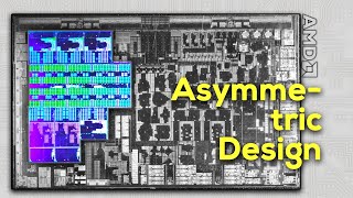
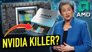
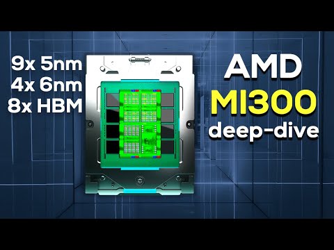
AMD's MI300 combines five next-gen technologies into one 147 billion transistor chip monster. In this video we will take a closer look at the tech AMD uses to combine CDNA3 GPU cores with Zen 4 CPU cores to create the worlds first HPC AI APU and talk about AMD's strategy for reaching Zettascale in the future.
Support me on Patreon: https://www.patreon.com/user?u=46978634
Follow me on Twitter: / highyieldyt
0:00 Intro
0:42 Five next-gen technologies of MI300
3:19 MI300 Specs
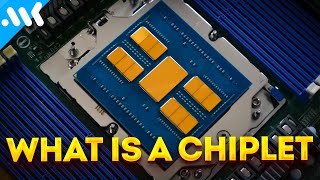
4:36 Chiplet Design
8:06 Brilliant
9:15 Advanced Packaging / 3D Stacking
11:48 SoC / APU Design
13:15 Unified Memory
14:16 AI / ML Acceleration
15:15 AMD's Zettascale Strategy